The ESP-12F is the module version of the ESP8266 chip. It has a built-in antenna, flash memory, and breaks out most of the useful GPIO pins. It is cheap, widely supported, and perfect for adding WiFi to a custom PCB without dealing with the bare chip.
This walkthrough covers designing a custom carrier board for the ESP-12F in KiCad from scratch — schematic, footprint, layout, and the mistakes worth avoiding.
What the ESP-12F Needs to Run
Before touching KiCad, understand what the module actually needs:
- 3.3V power — the ESP-12F runs on 3.3V only. No 5V tolerance.
- 100–500 mA peak current — WiFi transmission causes large current spikes. Your regulator and decoupling capacitors must handle this.
- Boot mode pins — GPIO0, GPIO2, and GPIO15 determine boot mode and must be pulled correctly at startup.
- EN pin — must be pulled high to enable the chip.
- RST pin — pulled high for normal operation, pull low to reset.
Boot Mode Pin Configuration
This is the most important thing to get right. Get it wrong and the module either refuses to boot or boots into the wrong mode.
| Pin | Normal Boot | Flash Mode |
|---|---|---|
| GPIO0 | Pull HIGH (10kΩ) | Pull LOW |
| GPIO2 | Pull HIGH (10kΩ) | Pull HIGH |
| GPIO15 | Pull LOW (10kΩ) | Pull LOW |
| EN | Pull HIGH (10kΩ) | Pull HIGH |
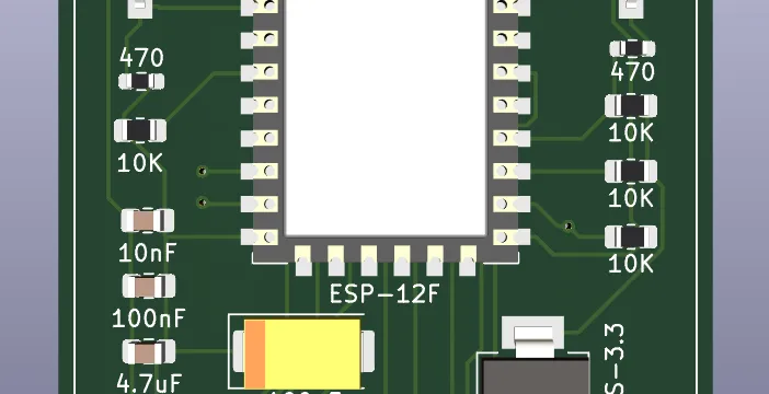
For a production board, wire GPIO0 and GPIO2 high with 10kΩ resistors, GPIO15 low with a 10kΩ resistor. Add a button that pulls GPIO0 low for firmware flashing.
Power Supply Design
The ESP-12F draws up to 250 mA average and can spike to 500 mA during WiFi transmission. This kills weak regulators and causes resets if your decoupling is poor.
Use the AMS1117-3.3 or XC6206 regulator. Add at minimum:
- 10 µF electrolytic capacitor on the 3.3V rail
- 100 nF ceramic capacitor as close as possible to the ESP-12F VCC pin
- Another 100 nF ceramic on the regulator output
Skipping the decoupling capacitors is the single most common reason an ESP-12F board works on a bench supply but resets randomly in real use.
Creating the Schematic in KiCad
Step 1 — Add the ESP-12F symbol
The ESP-12F symbol is not in the default KiCad library. You have two options:
- Download it from SnapEDA or Component Search Engine
- Draw it yourself (takes about 10 minutes and is good practice)
To draw it yourself: open the Symbol Editor, create a new symbol, add pins matching the ESP-12F datasheet pinout. Name them exactly as in the datasheet — this helps when cross-referencing later.
Step 2 — Wire the supporting components
Add these components to your schematic:
- Voltage regulator (AMS1117-3.3)
- Input capacitor 10 µF
- Output capacitors — one 10 µF electrolytic, two 100 nF ceramic
- 10kΩ pull-up resistors for GPIO0, GPIO2, EN
- 10kΩ pull-down resistor for GPIO15
- Reset button
- Flash button (pulls GPIO0 low)
- Programming header — TX, RX, GND, 3.3V, GPIO0, RST
Step 3 — Add power flags
KiCad’s ERC (Electrical Rules Check) will complain about power pins not driven unless you add PWR_FLAG symbols to your VCC and GND nets. Add one PWR_FLAG to each power net to silence these warnings.
Run the ERC before moving to layout. Fix every error — do not ignore them.
PCB Layout in KiCad
Footprint for the ESP-12F
The ESP-12F has 22 pads on 2mm pitch around three sides of the module. The pad size is 0.9mm x 1.6mm with 2mm center-to-center spacing.
If you downloaded the footprint, verify it against the datasheet before using it. Community footprints sometimes have wrong pad sizes or spacing.
The ESP-12F also needs a keep-out area under the metal shield for copper pours. Add a courtyard that covers the full module area and set a no-copper-fill rule under it.
Layout Tips
Antenna clearance — the ESP-12F has a PCB antenna built in. Keep all copper, components, and ground planes at least 3mm away from the antenna end of the module. Copper near the antenna detunes it and kills range.
Decoupling capacitor placement — the 100 nF ceramic caps must be as close as physically possible to the VCC pin of the ESP-12F. Every millimeter of trace between the cap and the pin adds inductance and reduces effectiveness.
Programming header — place it on an edge of the board so you can access it with a clip or header without removing the board from an enclosure.
Button placement — the flash button only needs to be accessible during development. You can place it anywhere convenient. The reset button is more useful in production so put it somewhere accessible.
Ground Plane
Use a ground plane on the bottom layer. In KiCad, use the copper fill tool and set the net to GND. Run DRC after filling to check for clearance violations.
The ground plane helps with signal integrity and gives your bypass capacitors a low-inductance return path.
Design Rule Check
Before sending to fab, run the DRC in KiCad and fix every error. Common issues:
- Traces too close to each other
- Pads not connected (missing ratsnest connection)
- Copper too close to board edge
- Silkscreen overlapping pads
Set your DRC rules to match your fab’s capabilities. For JLCPCB standard: minimum trace width 0.127mm, minimum clearance 0.127mm, minimum drill 0.3mm.
Generating Gerbers
In KiCad’s PCB editor: File → Fabrication Outputs → Gerbers. Use these layers:
- F.Cu, B.Cu (copper layers)
- F.Mask, B.Mask (solder mask)
- F.Silkscreen, B.Silkscreen
- Edge.Cuts (board outline)
- F.Paste (if using SMT assembly)
Also export the drill file. Zip everything together and upload to your fab.
Common Mistakes Summary
- No decoupling caps → random resets under WiFi load
- Wrong boot pin configuration → module won’t boot or flashing fails
- Copper under antenna → poor WiFi range
- Weak regulator → voltage sag during transmission causes resets
- Missing PWR_FLAG → false ERC errors that hide real ones
The ESP-12F is a solid module once the support circuitry is right. Most problems come from cutting corners on power supply design or ignoring the boot pin requirements.